Lee group
Materials Science and NanoEngineering at Rice University, Houston
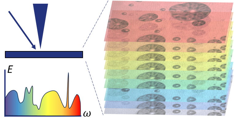
See, quantify, and manipulate electronic states by spatially resolved spectroscopy for programmable devices

Latest News
02/2026
New article out in Nano Letters! We shows stacking faults in hBN can easily form during mechanical handling
and they locally degrade dielectric strength of hBN. Rice News
09/2025
New article out in Nano Letters! We developed an approach to deterministically control optical emission
and conductivity of vdW oxide by using electron-beam. Rice News
09/2025
Zeming and Meer joined group! Welcome!
07/2025
Hyunchul joined group as a RAMI Postdoctoral Fellow! Welcome!
06/2025
New article out in Nature Photonics! We demonstrate waveguide quantum electrodynamics in van der Waals
heterostructures, using infrared nano-photoluminescence to probe how emitters couple to highly confined
waveguide modes.
01/2025
New article out in The Journal of Physical Chemistry C! HaeYeon is corresponding author of the paper.
We demonstrated p-type monolayer MoTe2 transistor by interfacial charge transfer doping.
Read all news here.
Research
Lee group focuses on exploring optoelectronic and photonic properties of low-dimensional quantum materials
at nanoscale to control their properties in desired way and to develop devices for next generation electronic
nd information technology. We specialize in scanning microscopy (using electrons, photons, and metallic tip
as probes) that enables us to see the atoms and their nanostructures, touch and move them.
Design quantum materials
There are various degrees of
freedom to manipulate material
properties including strain, doping,
and interlayer coupling. We are
aiming to develop new techniques
to synthesize and manipulate the
materials with high precision and
controllability.

Spatially resolved spectroscopy
with high spatial- and energy-
resolution is a powerful
characterization tool to visualize
microscopic nature of quantum
materials. We are aiming to reveal
new physical phenomena that
originate all the way down to single
atom level.
Comprehensive understanding,
from the atomic to the device level,
is essential for realizing programmable
electronic states and devices. Using
state-of-the-art device fabrication
techniques, we are aiming to build next-generation optoelectronic,
neuromorphic device platforms.

Bulk measurements such as electrical transport average the responses over the entire sample (global measurement). Spatially resolved
imaging reveals more details on how each part of sample varies (local measurement). Our goal is to bridge the gap between global and
local measurements, thereby contributing to the advancement of the scientific community of growth, characterization, and theoretical
framework development.
Group
HaeYeon Lee

Assistant Professor
and Principal Investigator
haeyeonlee@rice.edu
Postdoc. 2021-2023
Hone group, Columbia University
PhD 2021
Ross group & Gradečak group, MIT
Yifeng Liu

Postdoctoral Research Scientist
yl160@rice.edu
PhD 2024
Lou group, Rice University
Tian Lang

Graduate Student
tl153@rice.edu
BS Material Science and Engineering
Beijing University of
Chemical Technology, China
Aryan Chugh

Graduate Student
ac308@rice.edu
BS Physics (Applied)
Texas Tech University
Hyunchul Kim

RAMI Postdoctoral Fellow
hk82@rice.edu
co-advised by Prof. Jun Lou
PhD 2025
van der Zande group, UIUC
Zeming He

Graduate Student
zh72@rice.edu
MS 2025 Upenn
BS Chemical Engineering
Penn State University
Meer Mahfuz

Graduate Student
NSF Graduate Research Fellow
mm378@rice.edu
BS Materials Science and Engineering
University of Florida
Read more about group members: here.
Our sponsors
Selected Publications
Lang, T.*, Liu, Y.*, Chugh, A., Watanabe, K., Taniguchi, T., and Lee, H.Y. (2026) Hidden Stacking Fault Charge Traps in Hexagonal Boron Nitride and Their Impact on Dielectric Breakdown. Nano Letters, online. link
Liu, Y., Luo, S., Wu, W., Murakami, F., Lang, T., Chugh, A., Lin, C., Watanabe, K., Taniguchi, T., Huang, S., Zhao, Y., Lou, J., and Lee, H.Y. (2025) Spatial control of optical emission and conductivity in molybdenum oxide through electron beam irradiation. Nano Letters, 25, 36, 13664–13671. link
Moore, S. L., Lee, H. Y., Rivera, N. , Karube, Y. , Ziffer, M., Yanev, E. S. , Darlington, T. P. , Sternbach, A. J., Holbrook, M. A., Pack, J., Xu, X., Dean, C. R., Owen, J. S., Schuck, P. J. , Delor, M. Zhu, X. Y., Hone, J. & Basov, D. N. (2025). Van der Waals waveguide quantum electrodynamics probed by infrared nano-photoluminescence. Nature Photonics, 19, 833-839. link
Lee, H. Y., Wang, Z., Chen, G., Holtzman, L. N., Yan, X., Amontree, J., … & Hone, J. C. (2024). In situ via Contact to hBN-Encapsulated Air-Sensitive Atomically Thin Semiconductors. ACS Nano. 18, 26, 17111–17118
Lee, H. Y., Sarkar, S., Reidy, K., Kumar, A., Klein, J., Watanabe, K., … & Gradečak, S. (2022). Strong and Localized Luminescence from Interface Bubbles Between Stacked hBN Multilayers. Nature Communications, 13(1), 5000.
Reidy, K., Thomsen, J. D., Lee, H. Y., Zarubin, V., Yu, Y., Wang, B., … & Ross, F. M. (2022). Mechanisms of quasi van Der waals epitaxy of three-dimensional metallic nanoislands on suspended two-dimensional materials. Nano Letters, 22(14), 5849-5858.
Bonnet, N., Lee, H. Y., Shao, F., Woo, S. Y., Blazit, J. D., Watanabe, K., … & Tizei, L. H. (2021). Nanoscale modification of WS2 trion emission by its local electromagnetic environment. Nano Letters, 21(24), 10178-10185.
Lee, H. Y., Al Ezzi, M. M., Raghuvanshi, N., Chung, J. Y., Watanabe, K., Taniguchi, T., … & Gradecak, S. (2021). Tunable optical properties of thin films controlled by the interface twist angle. Nano Letters, 21(7), 2832-2839.
Lee, H. Y., Kim, S., Park, J. Y., Oh, Y. W., Park, S. Y., Ham, W., … & Park, B. G. (2019). Enhanced spin–orbit torque via interface engineering in Pt/CoFeB/MgO heterostructures. APL Materials, 7(3).
Oh, Y. W., Chris Baek, S. H., Kim, Y. M., Lee, H. Y., Lee, K. D., Yang, C. G., … & Park, B. G. (2016). Field-free switching of perpendicular magnetization through spin–orbit torque in antiferromagnet/ferromagnet/oxide structures. Nature nanotechnology, 11(10), 878-884.
